Navigation
- next
- previous |
-
leaflabs.com ·
- Index »
This page is a general resource for information specific to the Maple.
Contents
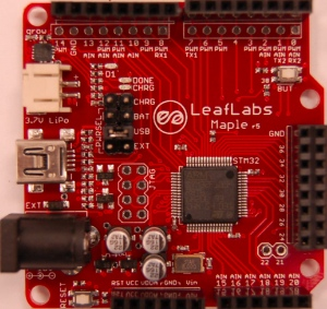
We went through three versions (“Revs”) of the Maple hardware: Rev 1, Rev 3, and Rev 5 [1]; Rev 5, the final design, is currently on sale. The following sections will help you to help you identify your Rev.
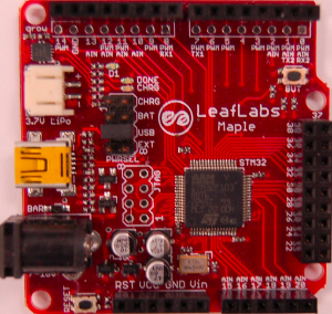
These boards went on sale in November 2010. They have white buttons and “r5” in small print near the “LeafLabs Maple” text next to the “infinity leaf” logo. The Maple Rev 5 repositioned the double header on the right hand side to better fit 0.1 inch pitch breadboard. This necessitated the removal of pins 21 and 22 from the double header; they are still available, but don’t have any headers installed on them.
The Maple’s power source is determined by the header to the left of the “LeafLabs” label on the silkscreen. All versions of the Maple can be powered from the barrel jack connector, USB, or a LiPo battery. We ship the Maple with a jumper on the USB selector. In order to power it off of an alternative source, unplug the Maple, then move the jumper to the desired selector before reconnecting power.
You can also power the Maple via the pin labeled “Vin” on the lower header. This pin feeds into both the digital and analog voltage regulators. However, don’t do this while simultaneously powering the board from another source, or you could damage it.
When powering the board from a barrel jack, double check the polarity of the barrel. The appropriate polarity is noted on the silkscreen right next to the connector.
Warning
Silkscreens on Maples up through Rev 5s manufactured in Spring 2011 falsely indicated that the barrel jack could be supplied by up to 18V. (Rev5s manufactured after Spring 2011 may still have this error on the silk, but it has been marked over.) We recommend a barrel jack input voltage no greater than 12V, and potentially even lower depending upon the current draw requirements of the application. The same goes for powering off LiPo batteries.
Please see Power Regulation on the Maple for more information.
Power regulation on the Maple is provided by two low dropout linear voltage regulators. (The part is the MCP1703 from Microchip, in the SOT-23A package. You can download the datasheet here ). One of the regulators supplies power to the digital voltage plane; the other supplies power to the analog voltage plane.
These voltage regulators nominally take an input of up to 16V. In addition, while the maximum continuous output current for the board is 250mA, if you are powering the board off higher voltages the current it can supply goes down, due to the regulators needing to dissipate the extra power. So if you are powering the board off 12V, the max current is about 40mA at room temperature. In general (again, at room temperature) the max power dissipation (PD) for the chip is about .37W, and output current = PD/(Vin-Vout). For exact max current calculations, please refer to the datasheet linked above.
If you are planning to draw a lot of current from the Maple board, it is necessary to provide input power as close to 3.3V as possible. Powering the microcontroller circuitry and LEDs on the board alone takes approximately 30mA, so if you are powering the board with 12V that leaves only 10mA (at best) available for powering any user circuitry. Attempting to draw more than 10mA runs the risk of shorting out the power regulators and bricking your board.
Maples Rev 3 and Rev 5 also have a built-in LiPo battery charger. In order to use it, put a jumper across the CHRG header on the power selection header and across the USB, or EXT selectors, depending on whether you’re charging the battery via USB cable or barrel jack connector. The LED labeled CHRG will light up while the battery is being charged. When the battery is finished charging, the LED labeled DONE will light up.
The Maple features 38 ready-to-use general purpose input/output (see GPIO) pins for digital input/output, numbered D0 through D37. These numbers correspond to the numeric values next to each header on the Maple silkscreen.
Pin D38 is the board’s button pin. It is thus mainly useful as an input. The pin will read HIGH when the button is pressed.
More GPIOs (numbered D39–D42 on the back of the Maple’s silkscreen) are available if you use the disableDebugPorts() function; see the board-specific debug pin constants for more information. (See this erratum for information about the pin numbered 43 on the silkscreen).
This table shows a summary of the available functionality on every GPIO pin, by peripheral type. The “5 V?” column documents whether or not the pin is 5 volt tolerant.
Note that this table is not exhaustive; on some pins, more peripherals are available than are listed here.
| Pin | GPIO | ADC | Timer | I2C | UART | SPI | 5 V? |
|---|---|---|---|---|---|---|---|
| D0 | PA3 | CH3 | 2_CH4 | 2_RX | |||
| D1 | PA2 | CH2 | 2_CH3 | 2_TX | |||
| D2 | PA0 | CH0 | 2_CH1_ETR | 2_CTS | |||
| D3 | PA1 | CH1 | 2_CH2 | 2_RTS | |||
| D4 | PB5 | 1_SMBA | |||||
| D5 | PB6 | 4_CH1 | 1_SCL | Yes | |||
| D6 | PA8 | 1_CH1 | 1_CK | Yes | |||
| D7 | PA9 | 1_CH2 | 1_TX | Yes | |||
| D8 | PA10 | 1_CH3 | 1_RX | Yes | |||
| D9 | PB7 | 4_CH2 | 1_SDA | Yes | |||
| D10 | PA4 | CH4 | 2_CK | 1_NSS | |||
| D11 | PA7 | CH7 | 3_CH2 | 1_MOSI | |||
| D12 | PA6 | CH6 | 3_CH1 | 1_MISO | |||
| D13 | PA5 | CH5 | 1_SCK | ||||
| D14 | PB8 | 4_CH3 | Yes | ||||
| D15 | PC0 | CH10 | |||||
| D16 | PC1 | CH11 | |||||
| D17 | PC2 | CH12 | |||||
| D18 | PC3 | CH13 | |||||
| D19 | PC4 | CH14 | |||||
| D20 | PC5 | CH15 | |||||
| D21 | PC13 | ||||||
| D22 | PC14 | ||||||
| D23 | PC15 | ||||||
| D24 | PB9 | 4_CH4 | Yes | ||||
| D25 | PD2 | 3_ETR | Yes | ||||
| D26 | PC10 | Yes | |||||
| D27 | PB0 | CH8 | 3_CH3 | ||||
| D28 | PB1 | CH9 | 3_CH4 | ||||
| D29 | PB10 | 2_SCL | 3_TX | Yes | |||
| D30 | PB11 | 2_SDA | 3_RX | Yes | |||
| D31 | PB12 | 2_SMBA | 3_CK | 2_NSS | Yes | ||
| D32 | PB13 | 3_CTS | 2_SCK | Yes | |||
| D33 | PB14 | 3_RTS | 2_MISO | Yes | |||
| D34 | PB15 | 2_MOSI | Yes | ||||
| D35 | PC6 | Yes | |||||
| D36 | PC7 | Yes | |||||
| D37 | PC8 | Yes | |||||
| D38 | PC9 | Yes | |||||
| D39 | PA13 | Yes | |||||
| D40 | PA14 | Yes | |||||
| D41 | PA15 | Yes | |||||
| D42 | PB3 | Yes |
The following table shows what pins are associated with each GPIO port.
| GPIOA | GPIOB | GPIOC |
|---|---|---|
| PA0: D2 | PB0: D27 | PC0: D15 |
| PA1: D3 | PB1: D28 | PC1: D16 |
| PA2: D1 | PB2: - | PC2: D17 |
| PA3: D0 | PB3: D42 | PC3: D18 |
| PA4: D10 | PB4: D43 | PC4: D19 |
| PA5: D13 | PB5: D4 | PC5: D20 |
| PA6: D12 | PB6: D5 | PC6: D35 |
| PA7: D11 | PB7: D9 | PC7: D36 |
| PA8: D6 | PB8: D14 | PC8: D37 |
| PA9: D7 | PB9: D24 | PC9: D38 |
| PA10: D8 | PB10: D29 | PC10: D26 |
| PA11: - | PB11: D30 | PC11: - |
| PA12: - | PB12: D31 | PC12: - |
| PA13: D39 | PB13: D32 | PC13: D21 |
| PA14: D40 | PB14: D33 | PC14: D22 |
| PA15: D41 | PB15: D34 | PC15: D23 |
The following table shows what pins are associated with a particular timer’s capture/compare channels.
| Timer | Ch. 1 | Ch. 2 | Ch. 3 | Ch. 4 |
|---|---|---|---|---|
| 1 | D6 | D7 | D8 | |
| 2 | D2 | D3 | D1 | D0 |
| 3 | D12 | D11 | D27 | D28 |
| 4 | D5 | D9 | D14 | D24 |
The following table shows which pins connect to which EXTI lines on the Maple.
| EXTI Line | Pins |
|---|---|
| EXTI0 | D2, D15, D27 |
| EXTI1 | D3, D16, D28 |
| EXTI2 | D1, D17, D25 |
| EXTI3 | D0, D18, D42 |
| EXTI4 | D10, D19 |
| EXTI5 | D4, D13, D20 |
| EXTI6 | D5, D12, D35 |
| EXTI7 | D9, D11, D36 |
| EXTI8 | D6, D14, D37 |
| EXTI9 | D7, D25, D28 |
| EXTI10 | D8, D26, D29 |
| EXTI11 | D30 |
| EXTI12 | D31 |
| EXTI13 | D21, D32, D39 |
| EXTI14 | D22, D33, D40 |
| EXTI15 | D23, D34, D41 |
The Maple has three serial ports (also known as USARTs): Serial1, Serial2, and Serial3. They communicate using the pins given in the following table.
| Serial Port | TX | RX | CK | CTS | RTS |
|---|---|---|---|---|---|
| Serial1 | D7 | D8 | D6 | ||
| Serial2 | D1 | D0 | D10 | D2 | D3 |
| Serial3 | D29 | D30 | D31 | D32 | D33 |
The six pins at the bottom right of the board (D15—D20) generally offer lower-noise ADC performance than other pins on the board. If you’re concerned about getting good ADC readings, we recommend using one of these pins to take your measurements.
Maple has an electrically isolated analog power plane with its own regulator, and a geometrically isolated ground plane. Pins D15—D20 are laid out to correspond with these analog planes, and our measurements indicate that they generally have the lowest noise of all the analog lines. However, analog performance may vary depending upon the activity of the other GPIOs. Consult the Maple hardware design files for more details.
This section lists the Maple’s board-specific values.
The hardware schematics and board layout files are available in the Maple GitHub repository. The design files for Rev 1, Rev 3, and Rev 5 are respectively in the maple-r1, maple-r3, and maple-r5 subdirectories. A schematic for a JTAG adapter suitable for use with Maple is available in the jtagadapter directory.
From the GitHub repository main page, you can download the entire repository by clicking the “Download” button. If you are familiar with Git, you can also clone the repository at the command line with
$ git clone git://github.com/leaflabs/maple.git
The following are known failure modes. The failure modes aren’t design errors, but are easy ways to break or damage your board permanently.
This section documents design flaws and other errors.
The following subsections lists known issues and warnings for each revision of the Maple board.
ADC noise: generally very high, in particular when the USB port is being used for communications (including keep-alive pings when connected to a computer).
This issue was resolved in Rev 3 with a 4-layer design and a geometrically isolated ADC Vref plane.
Resistors on pins 0 and 1: these header pins, which are RX/TX on USART2 (Serial2), have resistors in-line between the STM32 and the headers. These resistors increase the impedance of the lines for ADC reads and affect the open drain GPIO functionality of the pins.
These resistors were accidentally copied over from older Arduino USB designs, where they appear to protect the USB-Serial converter from TTL voltage on the headers.
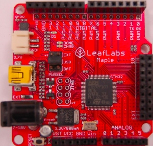
Silkscreen Differences: the pin numbering scheme on Rev 1 is different from Rev 3, and thus Rev 3 software is difficult to use with Rev 1 boards. Notably, the analog input bank is labeled A0-A4 on Rev 1 but 15-20 on Rev 3, and the extra header bank does not have a pinout table on the bottom.
No BUT Button: the BUT button, useful for serial bootloading, was only added in Rev 3. As a workaround, you can directly short the appropriate MCU pin to Vcc; see this forum posting.
STMicro documentation for STM32F103RB microcontroller:
Footnotes
| [1] | Revs 2 and 4 were prototypes that didn’t pass internal testing. |